Based on materials from Nikkei
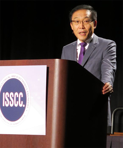
Dr. Kinam Kim, head of semiconductor manufacturing at Samsung, spoke at the IEEE International Solid-State Circuits Conference (ISSCC), announcing global plans for the development of this direction. According to him, at the moment, a trend is developing for further miniaturization of production and the transition to ever smaller chipsets. He announced this at a lecture on Silicon Technologies and Solutions for The Data-driven World.
According to Dr. Kim, the world is currently dominated by huge flows of information and data, as well as the IoT (Internet of Things). Even last year, according to Cisco Systems, Inc., there were 7.2 billion people in the world, but they used twice as many devices connected to the Internet, that is, approximately 14.4 billion different gadgets that can go online. By 2020, that number will grow to 50 billion devices.
Such an increase in the number of connected terminals causes an increase in the number of connections, which also entails an increase in the number of processed signals. All of this requires a corresponding growth in semiconductor technology that would support development. And this development of semiconductors has a good start. At the moment, “there are no major technical difficulties to reach the 5nm milestone,” said Kinam Kim.
But the company will not stay at the 5 nm line either. The already developed FinFET technology, so far adapted for the 10 nm process technology, makes it possible to create research prototypes using the 3.8 nm process technology, and in the future, it is possible to switch to EUV technology, which could realize the size of 3.25 nm. In the meantime, its use is limited to the 8nm technical process, and new materials are required for further miniaturization.
However, all of the above is still a matter for the next few years. So far, Samsung began in January 2015 mass production of chipsets of the FinFET generation of technology with a 14nm process technology. The nearest plans are to achieve the 7 nm level within this technology and master TFET technologies in serial production.